Leading the Future of
ESD & Latch-up Testing
iTest Inc. redefines ESD and Latch-up Testing—delivering uncompromising reliability and performance for the most advanced semiconductor technologies. From wafer-level characterization to final production test, one partner covers it all.

Dedicated ASIC’s ESD & Latch-up
Testing Services
iTest Inc. powers your product success with visionary technology, integrated processes, innovative test layouts, seamless interconnect environments, and breakthrough capabilities.
Two Categories. One Complete Solution.
Not all Latch-up is the same. Modern ASICs and high-power devices demand a completely different testing approach than standard CMOS logic. iTest covers both.
Standard Latch-up originates from parasitic PNP/NPN bipolar transistor pairs inherent in CMOS structures. When triggered — by current injection on an I/O pin, an overvoltage spike, or an ESD event — these parasitic transistors form a low-impedance SCR path between VDD and GND, causing destructive current flow. Standard testing per JESD78F requires injecting ±100 mA trigger current into each I/O pin and verifying the device does not sustain an elevated current state (Inom > 25mA → failure threshold ≥ 1.4× Inom).
Why Reliability Testing Cannot Be Skipped
A device that passes functional test can still fail in the field. Reliability testing finds the failure modes that only appear under real operating stress — before your product ships.
Latch-up remains a top reliability concern for devices targeting less than 1% field failure rates. Automotive, medical, and aerospace applications require demonstrated immunity across the full operating voltage, temperature, and current envelope before qualification.
Junction temperature directly affects latch-up susceptibility. Our real-time thermal management system controls die temperature throughout every test pulse — ensuring results reflect actual chip operating conditions, not bench conditions.
Every test captures supply currents, hold voltages, trigger responses, and device behavior in real time. Full data logs in ASCII and Excel formats. Every failure mode is visible, traceable, and actionable — not just a pass/fail result.
Multi-voltage devices are especially vulnerable during power-up sequences when some rails are active before others. We replicate exact power-up/down sequences to expose latch-up conditions that only arise during system initialization.
Transient latch-up triggered by ESD events or supply voltage spikes is a leading cause of field returns. Our programmable slew rates, ramp rates, and overvoltage spike simulation expose vulnerabilities before they become product recalls.
AEC-Q100 qualification mandates full latch-up testing across the complete automotive temperature range. Our junction temperature regulation system ensures tests are performed at exactly the specified conditions — repeatable, traceable, auditable.
See Our Technology at Work
Watch how our iTest proprietary test IP and in-house equipment come together for ESD, Latch-up, and Final Test flows.
Why Your Equipment Choice
Matters More Than Ever
Not all ESD and Latch-up testers are created equal. As semiconductor devices grow more complex, legacy relay-based architectures simply cannot keep up. See how the options stack up.
⚠ Legacy Systems Are Holding You Back
The Keytek MK4—originally designed by Keytek, later acquired by Thermo Fisher Scientific—is a classic example of a platform left behind by corporate decisions. After the acquisition, the engineering team responsible for the machine's development was disbanded, leaving the product without meaningful roadmap updates. Today it runs on only 5 power supplies delivering a maximum of 18 Amperes—far below what modern high-performance, multi-rail chip designs require. Without sustained engineering investment, customer support is limited and updates have not kept pace with current semiconductor demands.
|
Keytek / Thermo Fisher MK4
Legacy · Discontinued Roadmap
Legacy |
Hanwa HED-G5000 Series
Hanwa Electronic Ind. — In-House
Active · In-House |
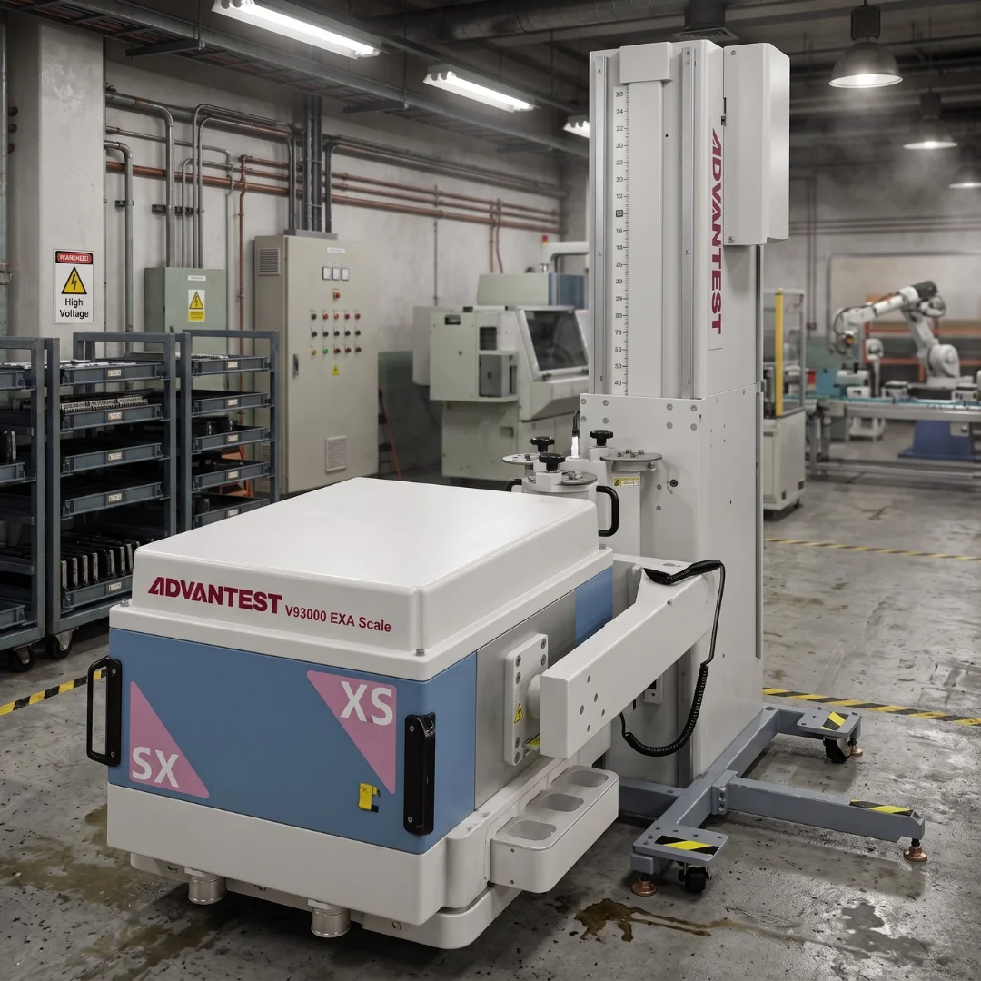
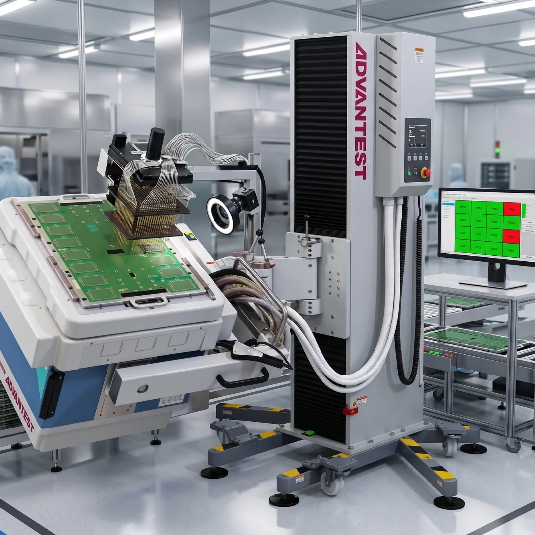
Advantest V93000 ATE
iTest Proprietary Test IP
★ Most Innovative |
|
|---|---|---|---|
| Power Supplies | 5 only Insufficient for modern complex devices |
Up to 6 Bias (D6) +/−35V standard; options to 100V |
64 Integrated Simulates complex real-world power rails |
| Max Current | 18A max | Up to 100A / rail +/−2V @ 100A option |
640A Ultra-high current for maximum load validation |
| Parasitic Design | High — Relay Matrix Large parasitic capacitors degrade waveform accuracy |
Ultra-Low Parasitic Mechanical design; ANSI/ESDA/JEDEC JS-001 compliant |
Ultra-Low Parasitic ATE-grade architecture; clean, precise waveforms |
| Pin Count | Limited | 256 / 512 / 768 / 1024 / 2048 | Any pin count in market |
| Test Vectors | Minimal Limits simulation depth |
Standard | Unlimited Deep Vectors Deep vector chains with loops |
| Temperature Control | Poor / Inadequate | Standard | Real-Time Junction Temp Control Active thermal management during stress |
| Final Test Capability | No | ESD / Latch-up only | Yes — Proprietary Test IP Full Final Test reusing same hardware |
| Vendor Roadmap | Discontinued / Abandoned Engineering team disbanded post-acquisition |
Active — Decades of updates Continuously evolving to market demand |
iTest Proprietary IP In-house developed & maintained software |
| Industry Adoption | Declining | Wafer Foundry Standard in Asia | Unique in the Market |
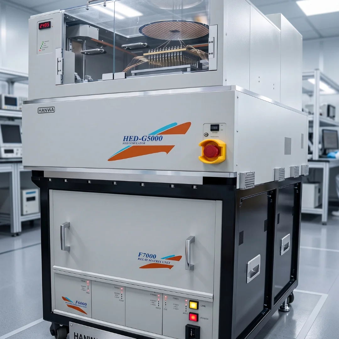
Hanwa HED-G5000
Ultra-Low Parasitic ESD & Latch-up
The Hanwa HED-G5000 series is the tester of choice for wafer foundries across Asia, routinely used in the production and assembly of modern wafers and chips. Unlike legacy relay-based designs where parasitic capacitance degrades waveform fidelity, the G5000 uses a patented mechanical rotating architecture that delivers ultra-low parasitic performance—cleaner results, higher accuracy, and true compliance with ANSI/ESDA/JEDEC JS-001-2017.
Hanwa Electronic Ind. Co., Ltd. has been designing and continuously updating this platform for decades, driven by real market demand—not acquisition decisions. We have this system here in-house, ready to serve your ESD and Latch-up testing needs with the same precision that TSMC, Samsung, and other leading foundries rely on.
Power Supply Options (G5000 Series)
Full Constant Correlation Advantest V93000 ATE
Next-Gen Ultra High Power Latch-up
ATE-grade architecture delivers cleaner, more reliable results with minimal electrical noise and resistance—critical for accurate ESD characterization.
64 integrated bias supplies simulate the complex multi-rail power environment of any real-world chip, from automotive to AI processors.
Enables greater accuracy, repeatability, and predictability. Supports transients, fast ramps, system-level scenarios, and fully programmable pulsing rates.
Real-time thermal management throughout the entire stress test sequence. Accurate junction temperature regulation prevents erroneous results.
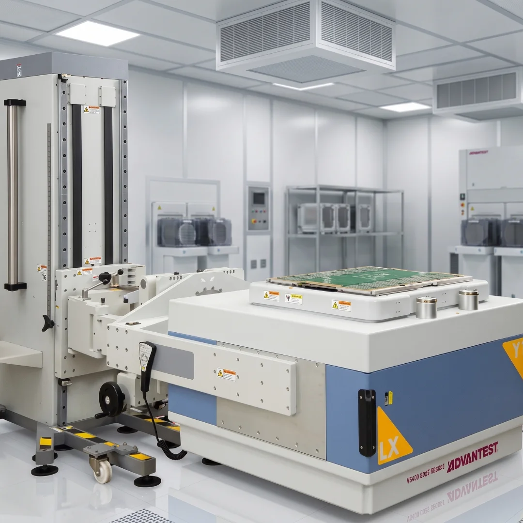

Multi-Rail Testing
Just Like a Real Chip Design
Our Latch-up testing supports multiple power rails at different voltages and current levels simultaneously—faithfully replicating the real-world operating conditions of modern SoCs, automotive ICs, and high-performance processors. Legacy systems with 3–4 power rails simply cannot match this fidelity.
Power Supplies
Total Current
Vector Depth
Pin Count
Accurate, Fast & Mission-Critical
Our testing infrastructure directly translates to better products, faster timelines, and higher confidence before your device ever reaches the field.
Cleaner and more reliable results thanks to ultra-low electrical noise and resistance. Critical for high-precision applications in automotive, aerospace, and medical. Finds hidden flaws early—the kind that only surface after a product ships.
With up to 64 separate power supplies, we faithfully simulate the complex power environment a chip faces inside a phone, automobile, or medical device—ensuring your device performs correctly in the real world, not just on a bench.
Spot issues faster, fix problems quicker, fewer delays. Identify subtle anomalies early to prevent costly field failures. Less setup time, fewer test repeats, more productivity—and a quicker path to production release.
Real-time monitoring of supply currents and device behavior during every stress event. Deep visibility into exactly how your device responds under each test condition.
Supports transients, fast ramps, and full system-level scenarios with fully programmable pulsing rates. Every edge case your chip might encounter, covered in a single engagement.
From wafer ESD characterization on the Hanwa G5000 to final production test on the Advantest V93000—iTest provides a seamless, fully integrated test flow with a single point of contact.
Seamless Integration Into
Your Existing Test Flow
The Advantest V93000 doesn't require you to rebuild your test program. Our proprietary IP reuses the same test environment as your Final Test, minimizing cost and time.
Reuse Final Test Programs
iTest uses the same test environment as your Final Test, with full compatibility for test cards, vector depths, and test routines—no rebuilding from scratch.
Simplified Setup
Custom load boards and specialized routing are tailored specifically to your device under test, reducing configuration time and eliminating setup uncertainty.
Real-Time Functional Testing
Monitor device performance during stress testing in real time. Ensures consistent, reliable results and allows immediate detection of anomalies before they propagate.
Industry-Wide Standard Compliance
Every test performed at iTest Inc. is executed in full conformance with globally recognized semiconductor reliability standards.
Concerned on True & Inaccurate Latch-Up Test Results?
Inquire Now
A failed Latch-up test is not the end — it's the beginning of a better design. Our engineers work with you to pinpoint the root cause, identify the vulnerable power rail or I/O domain, and validate the fix before your next tape-out. From first failure to final sign-off, iTest stays in your corner.